
Studying nanostructures at near-atomic resolution is the bread and butter of the ICMS Center for Multiscale Electron Microscopy. Here, Heiner Friedrich and his team are continuously improving these already advanced techniques to provide an even more accurate view with minimal noise and high throughput.
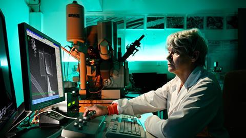
‘Microscopes really are the eyes of the scientist’, says physical chemist Heiner Friedrich, head of the Center for Multiscale Electron Microscopy (CMEM) at Eindhoven University of Technology. He and his team develop cryo-, in-situ & 3D electron microscopy (EM) approaches for the dynamic investigation of materials and their nanoscale features. These EM techniques form a crucial element in the work of many ICMS researchers who study (the synthesis of) complex structures. Friedrich: ‘We are providing more than 150 users with “very good eyes” to observe those structures at the range of nanometers to tens of micrometers.’
Electron microscopy mainly comes in two flavours: (1) detecting electrons that are emitted or reflected off the sample’s surface: scanning electron microscopy (SEM), or (2) measuring electrons that have passed through the sample: transmission electron microscopy (TEM). CMEM offers both techniques, with three SEMs and two TEMs. Friedrich: ‘We are a materials science lab that is also specialized in studying samples in their synthesis liquid, like water or organic solvent mixtures. Very few labs in the world do this.’
Counting electrons
To study (soft) nanostructures in their native solvent environment, researchers make use of cryo-EM. For this, a small droplet of the synthesis solution is placed on a TEM grid, then blotted into a very thin liquid film, and subsequently cooled down very rapidly to solidify into a glassy film. When working with organic solvent mixtures instead of water, these steps become extra challenging. ‘Water has a very well understood evaporation rate, but organic solvents may behave very differently’, says Friedrich. ‘We have gained the experience and created dedicated workflows to deal with this complexity.’
Continue reading below the photo
During the past ten years, multiple advancements have been achieved in the EM-field. For one, researchers have moved towards instruments that can load multiple cryo-samples at the same time. Friedrich: ‘Recently there has been a huge improvement in reproducibility and automation. In our microscope, we are now able to load a set of twelve cryo-samples and then choose which one to look at in more detail with a push of a button.’
Another improvement relates to detector technology. TEMs shoot electrons through a sample with a velocity of around two thirds the speed of light, thus carrying quite a punch. To prevent artifacts, the number of electrons should therefore be reduced to the required minimum. ‘Conventional cameras convert high energy electrons into light which is then channelled onto a chip. Instead, we now use a “direct electron detector”. This semiconductor device has an active layer that counts every single electron and determines where it hit the camera. That allows us to use fewer electrons, and it grants very precise images with less noise.’
Faster and faster
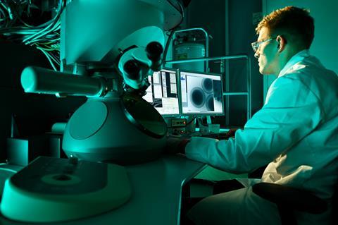
These advancements directly pay off for ICMS researchers. Bio-organic chemist Jianhong Wang develops nanovesicles as carriers to deliver therapeutic drugs into living cells. He uses cryo-TEM to study the different shapes and spatial distribution of his nanoparticles. Wang: ‘Cryo-EM requires the temperature to stay at liquid nitrogen level. I therefore load and run multiple samples at the same time, allowing for faster data acquisition.’
Another ICMS member, biochemist Nicoleta Ploscariu, uses cryo-TEM to study protein complexes. More specifically, she investigates the so-called 14-3-3 protein, which is highly involved in cell regulation and signalling. Using cryo-TEM, Ploscariu recently collected images of 14-3-3 interacting with a protein associated with Parkinson’s disease. ‘To investigate how this interaction happens, I reconstruct these protein complexes with near-atomic resolution’, Ploscariu explains. ‘In order to do this, I require close to ten thousand images. Nowadays, the TEM collects all these images in approximately two days, which a few years ago would have taken about a week.’
Three kilometers
To even further increase the data throughput, Friedrich aims to improve workflows: ‘We use automation to run the instruments sometimes in the evenings, overnight or in the weekend. However, users require specialized knowledge to handle this. By simplifying the workflows, we hope to make the technique more accessible to a larger audience.’
And there are more ways to Rome. ‘A TEM sample grid is three millimetres in diameter. When you think about it, this means that our microscopes – which magnify by a million times – enlarge samples to three kilometers, of which we see about 25 centimetres. We hope to use more of this available space, for example by placing multiple samples on the same grid.’


Nog geen opmerkingen